|
 |
Sales and Technical Support |
 |
 |
 |
 |
| |
SPCB Technical Advices |
|
Product Development :
|
|
During your product development, we might recommend on how to select raw material, design of layer structure etc. This is often done via Live Chart Support or email. |
|
Question: |
|
We seek out areas for your cost optimization, we may advise you on how to reduce the cost of your PCB fabrication may be lowered. For example, units arrangements in panel, lay-up design or a new panel design upon your reqeust and etc. |
|
Production Gerber file |
|
Once you confirm an order, we generate the production gerber file accroding to your orginal master file. We do fully design rule check (DRC) and inspect circuit pattern, each item against our process capablity and raise engineering question (EQ) if it's necessary. |
| What else we can do for you ? |
|
Technical Support
|
| |
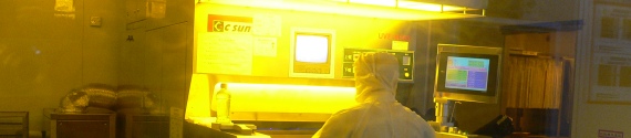
With massive oversea production, here are a couple of SPCB checking steps we do to avoid any technical difficulties upon the products’ arrival.
- Using the Gensiss CAM program to do visual inspection of the product to identify any production flaws
- Open for custom design for panel size, panel surface treatment and etc.
- Eliminate any information that could cause information leak and imprecise interpretations
- Verification and clarification on orders’ designs and requirements prior the mass production. For example, contour markings, tolerance of holes, contours and width of conductor.
- Instant Sample Quote
- Place Instant Online Order (for 24~36 hrs PCB manufacturing)
- Live Chart Support of Technical Queries
|
|
Technical Advice |
|
After we receive your design, we will first estimate the production cost and determine if the design is technically producible. Then, we will inform the customers’ total cost among any possible changes. In order to produce a perfect PCB for customers, slight modifications and changes are often necessary. Such as the space of the panel, ways of furnishing the surface, size of the layers, choices of the materials, methods of protection and the design of the layout. The procedure above can be explain or clarify in personal meetings and on phone as well. |
 |
Quotation terms |
|
|
For any engineering support, you may direct contact our customer service engineer at: info@standardpcb.com |
|
|
 |
|
 |
|