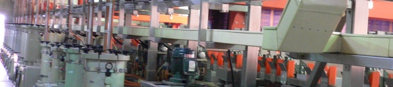
Description |
Technology & Capabilities |
1. |
Product Range |
  |
2 - 24 layers, HDI; Aluminium Based PCBs |
2. |
Base Material |
  |
FR-4 Glass Epoxy laminate, ALuminium Based (Others, by special order) |
3. |
Major Laminate |
  |
King Board (KB-6150/60), ShengYi (S1141, S1170), Rogers
High Frequency Materials: PTFE,Getek,Nelco (by order) |
4. |
Surface Finish Treatment |
  |
Flash gold (Electrolytic),
Electroless nickel Immersion gold (Electroless Ni/Au),
Organic Solderability Preservatives (OSP or Entek), Hot Air Leveling (=HAL-Tin/Lead),
Hot Air Leveling (Lead- Free, RoHS),
Carbon Ink, Peelable Mask. Gold Fingers (30µ"), Immersion Silver (3~10u"); Immersion Tin (0.6~1.2um) |
5. |
Via Holes |
  |
Copper PTH / Blind Via / Buried Via / HDI 2+N+2 with IVH |
6. |
Impedance l Control Tol. |
  |
+/-10% (min. +/-7 Ohm) |
7. |
Solder Mask |
  |
Liquid Photo-image (LPI) |
8. |
Profiling |
  |
CNC Routing, V-cutting, Punching, Push Back Punching, Connector chamfering |
9. |
Max. Board Size. |
  |
610 x 711mm (24" x 28") |
10. |
Min. Board Thickness. |
  |
0.2mm (2 layers) / 0.4mm (4 layers) / 0.9mm(8 layers) / 1.2mm (10 layers) / 1.3mm (12 layers) / 1.5mm (14 layers) / 1.7mm (16 layers) / 1.8mm / 2.0 mm (18 layers) / 2.2mm (20 layers) / 2.4mm ( 22 layers) / 2.6mm (24 layers) |
11. |
Copper Foil Thickness |
  |
18um / 35um / 70um ~ 245um (outerlayer:0.5oz~7oz)
18um / 35um / 70um ~ 210um (innerlayers:0.5oz~6oz) |
12. |
Min. Via Size and Type |
  |
Dia. 0.15mm (Finished);
Aspect Ratio = 12 ; HDI holes (<0.10mm) |
13. |
Min. Line width & Spacing |
|
0.10 mm / 0.10 mm (4 mil./ 4 mil.) |
14. |
Minimum via hole size and pad |
  |
via: dia. 0.2mm / pad: dia. 0.4mm ; HDI <0.10mm via |
15. |
Minimum hole tolerance |
  |
+/-0.05mm(NPTH), +/-0.076mm(PTH) |
16. |
Hole wall to Conductor |
Innerlayers of Multi-layers |
0.20mm |
17. |
Hole to Hole Edge Gap |
  |
0.8mm |
18. |
Minimum Tooling Hole
Diameter |
  |
1.5mm |
19. |
Minimum Legend Line
width |
  |
0.15mm |
20. |
Dimensional Tolerance |
  |
Punching:+/-0.1mm; PTH(+/-0.076mm) by drilling; NPTH(+/-0.05mm) by drilling; NPTH(+/-0.1mm) by punching; Remark: 6.0mm hole tolerance by routing is +/-0.13mm |
21. |
Other Dimensions |
Unless other specified |
Outline tolerance:+/-0.13mm for routing; +/-0.15mm for punching |
22. |
Minimum Annular Ring
|
The least circular strip plane of conductive material surrounding a hole |
Inner layer: / Outer layer: - Component holes: 0.2mm Via holes: 0.15mm |
23. |
Minimum Copper Trace
Width
|
The least noticeable width of the conductor in a circuit path on the printed wiring board |
Width/Spacing: 18um/0.5oz, 35um/1oz, 70um/2oz
Single Sided: 0.15mm, 0.15mm, 0.2mm |
24. |
Minimum Spacing
|
The least distance between adjacent edge of conductors (not-center-to-center)on a single layer of a printed wiring board. |
Double Sided: 0.10/0.13 mm, 0.13/0.13 mm, 0.2/0.2mm
Multilayer: 0.10/0.13 mm, 0.13/0.13 mm, 0.2/0.2mm
|
25. |
Minimum SMT Pitch
|
The least distance from center-to-center of adjacent conductive pads |
0.4mm |
26. |
Minimum Soldermask
Dam
|
The least width of soldermask between adjacent conductive pads |
Double sided: 0.25mm
Multilayer: 0.25mm
|
27. |
Minimum Soldermask
opening
|
Difference between pad width and soldermask opening |
Double sided: pad width 0.1mm
Multilayer: 0.075mm
|
28. |
Copper to Board Edge
Gap
|
The least distance between edge of conductors to the edge of the board |
0.4mm |
29. |
Copper to Hole Gap
|
The least distance between edge of conductors to the edge of the non-plated hole |
0.2mm |
30. |
Minimum Void/Thermal
Gaps
|
The least allowable non-copper contour inside a plane |
0.2mmX0.2mm or
(diameter=0.5mm) |
31. |
Acid Trap Closed
|
gap between two copper entities such as pad or trace |
0.2mm |
| 32. |
Capacity
|
  |
600,000 square feet (Month) |
Printed circuit boards require utmost precision in production and we provide the finest details of our capabilities to produce the world-class PCBs. The hole diameter, thickness of copper foil, material length, and other descriptions are needed to check very carefully against our process capablity, and this is where we spend our maximum effort. Check with our details provided above for various parameters.
Detail Manual of Process Capability
Aluminium base PCB Capability
|
|